Sputtering Services
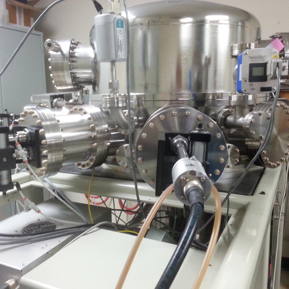
For your advanced materials research, a custom sputtering tool is available at Hi-Z. This tool is set up to fabricate unique structures. For example, Hi-Z’s proven sputtering system has grown repeatable alternating 10 nm layers of electrical conductors and 10 nm electrical insulators with >500 layers of each material. Also, semiconductor and metallic coatings have been applied to many different heated and unheated substrates to produce specific properties for distinctive applications.
Specifications for Hi-Z’s Sputtering System
Sputtering Sources
Four 3-inch Magnetron Sputtering Sources with Pneumatic Shutters (currently installed on the system or two 6-inch Magnetron Sources available for installation
Ultimate Base Vacuum: <1 x 10⁻⁷ Torr
Automatic Pressure Control by Control Valve
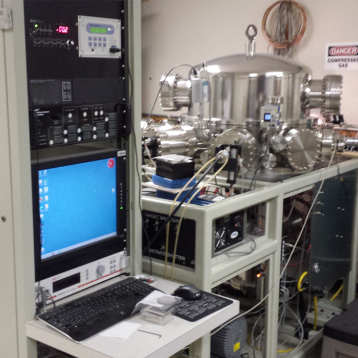
Source Power Supplies:
Two Pulse DC Power Supplies and two RF Power Generators with Automatic Impedance Matching Network
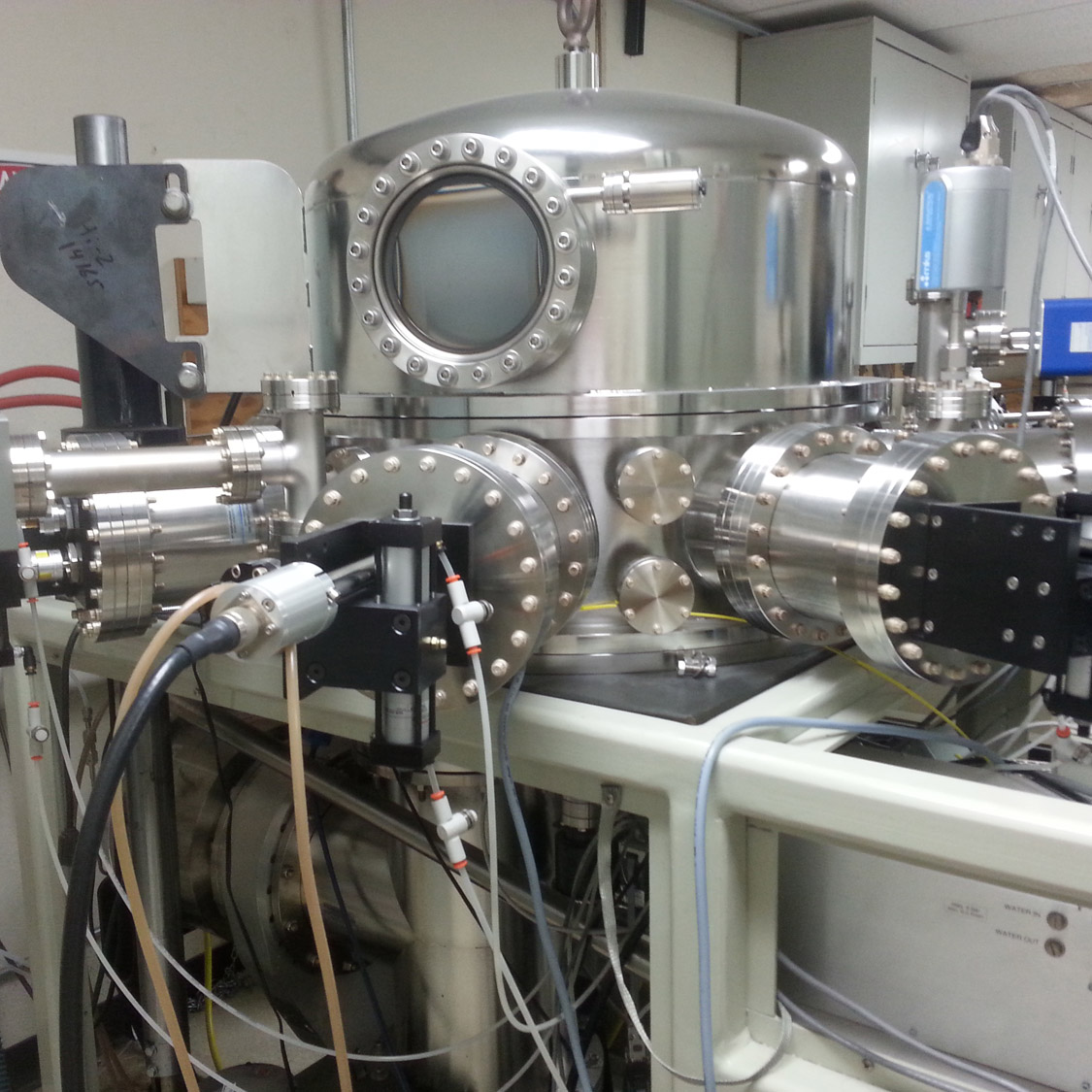
Substrates
Real Time Adjustable Substrate Orientation (i.e., sputtering source)
Substrate Heating (up to 650C) available for 2-inch or 6-inch circular wafers
Substrate Spinning Available with No Substrate Heating
Deposition Capability
Many different sputtering materials: Au, Si, SiGe, SiO2, SiC, B4,B9C, Si3N4, Mo, Bi2Te3, etc. and other materials upon request. Heated or unheated substrates: silicon, alumina, fused silica, aluminum nitride, including polymers such Kapton and Upilex and many other materials. In many thin film configurations: Single Layer, Multi-Layer, Periodic Structures, Composition Varying Structures and Coatings. In different sputtering modes: DC, Pulse DC, or RF Magnetron Sputtering.